One thing I’ve been procrastinating on for years is building a proper bench power supply. Minimally it needs a galvanically isolated single-ended DC output voltage adjustable from 0 V to 15 V with an adjustable current limit of up to at least a few hundred milliamps, some kind of readout that tells you what it’s delivering, and precision of ±10% or better over most of that range. Bipolarity supplies, larger voltages, very precise regulation, linear regulation, foldback current limiting, high efficiency, and thermal protection would be nice but are less essential.
The standard design for this kind of thing involves a lot of analog components, but computers are cheaper than transistors now, so it might be better to use an analog circuit that’s as simple as possible and pushes as much complexity as possible into software.
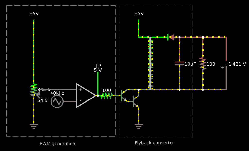
So ideally you’d like some kind of transformer-isolated switching buck–boost converter. Like a flyback converter, which I’ve drawn here being driven from a discrete-component PWM generation circuit instead of a microcontroller:
$ 1 1e-8 16.817414165184545 50 5 43 5e-11
R 208 160 160 160 0 3 40000 2.5 2.5 0 0.5
R 96 -48 96 -80 0 0 40 5 0 0 0.5
a 208 144 272 144 9 5 0 1000000 0.027999984128133537 0.025000000000000005 100000
174 96 192 112 64 1 1000 0.005 Resistance
g 96 192 96 224 0 0
w 112 128 208 128 0
368 272 144 272 64 0 0
t 320 144 352 144 0 1 -12.72087652079897 -0.20438741318712572 100 default
r 272 144 320 144 0 100
R 384 -16 384 -80 0 0 40 5 0 0 0.5
T 384 128 448 -16 0 0.000004 1 -3.0191582567340447e-10 -0.12340456006778311 0.999
d 496 -16 448 -16 2 1N5712
c 496 -16 496 128 0 0.000009999999999999999 -0.40177526518551265 0.001
w 496 128 448 128 0
w 496 -16 560 -16 0
w 496 128 560 128 0
r 560 -16 560 128 0 100
w 560 -16 624 -16 0
w 560 128 624 128 0
p 624 128 624 -16 1 0 0
w 96 64 96 -48 0
t 352 160 384 160 0 1 -12.516489107611845 0.2043871144711009 10 default
w 384 144 384 128 0
w 352 128 384 128 0
g 384 176 384 224 0 0
b 320 256 21 -103 0
x 112 280 210 283 4 12 PWM\sgeneration
b 332 -104 531 260 0
x 373 278 481 281 4 12 Flyback\sconverter
o 6 128 0 4099 10 6.4 0 2 6 3
o 19 128 0 4098 20 0.1 0 1
The actual flyback converter itself is four components: an npn darlington grounding one end of the primary of a transformer, a schottky, and a capacitor. Well, and a base resistor for the darlington if the input signal is voltage-mode PWM instead of current-mode PWM, so that’s five components. (Horowitz & Hill suggest a zener snubber across the primary to limit the voltage spike from the primary leakage inductance: a rectifier and a TVS zener, in opposite directions, so it’s more like seven. But I didn’t simulate that. In their example the leakage inductance is about 5% of the total.)
Here’s the values I chose in the above simulation:
With these values I get about:
At the top of the range (99.5% duty cycle) the output voltage is actually lower with this load.
It can drive thirstier loads like 10Ω at the cost of more ripple, for example 260–330 mV (±6%) but then it tops out at around 2.5–3.2 V (±6%), at which point it's pushing 300 mA (≈1 W). So you’d probably want a bigger output cap. τ = 10Ω·10μF = 100 μs, and the PWM period here is only 25 μs.
This design has a serious problem, though. At high output voltages, and especially when increasing the output voltage rapidly, the power transistor sucks up a lot of power, like tens to hundreds of watts. It seems that it’s not getting enough base current. At one point, for example, its Vce is 3.2 volts and its Ic is a rather alarming 33.6 amps, which wouldn’t be so bad if it had a nice saturated Vce of 0.2 volts or so, but noo, it’s forward active! It’s “only” getting 3.4 amps of base current, you see, because the other transistor is also forward active, because it’s only getting 33 mA of base current and so it’s “only” passing 3.4 amps of Ic. This is in part because both transistors have a relatively high Vbe at this point of almost 900 mV, reducing the voltage on the base resistor to only 3.3 V.
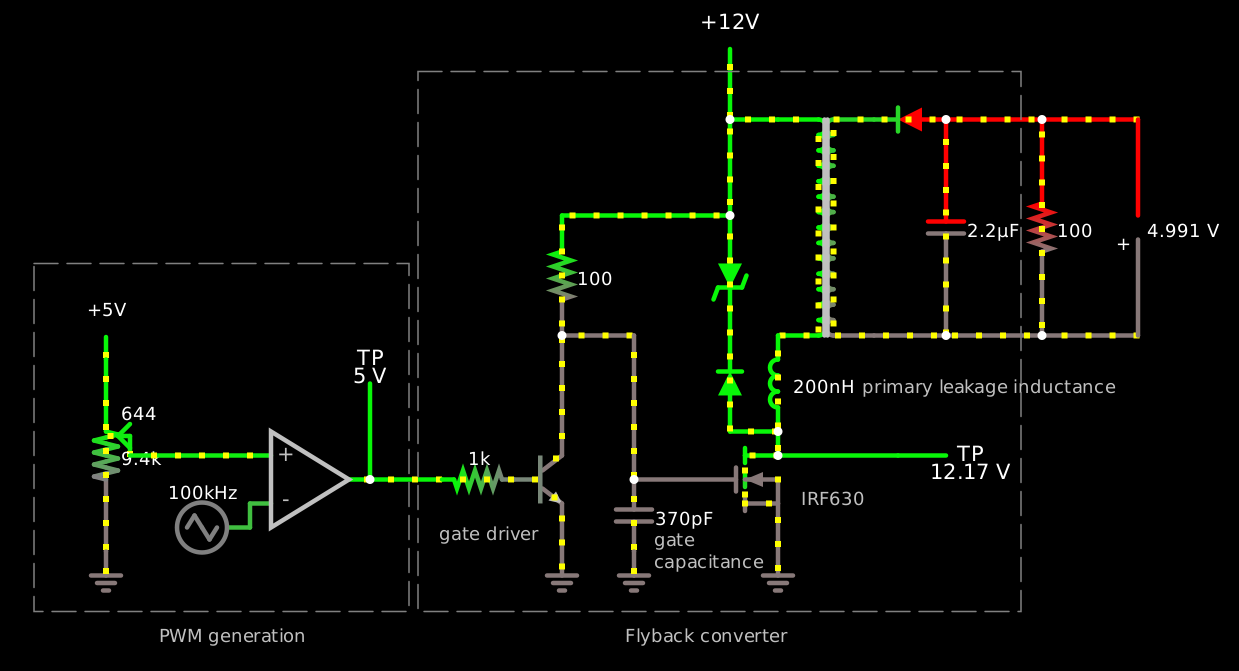
Reducing the base resistor value to 47 Ω helps a bit with the problem, but that’s demanding a lot of current on the PWM input. Even the 38 mA or so this circuit can demand is kind of a lot. Really probably what we need is an additional amplifier stage. Also it’s probably hard to find a transistor that can actually handle 3.4 amps of Ic but has β=100. A better alternative might be to use a pnp signal preamp (β=100) to drive an npn power darlington (β=10 × β=10); that way we avoid stacking more Vbes and can also use a beefy power transistor there. But using a power MOSFET, and maybe driving the whole circuit from a 12-volt supply instead of 5 volts so it can use lower currents, is maybe a better idea.
Doing the pnp-preamp thing driven from the PWM voltage input signal through a 470-Ω base resistor does indeed help keep the switching transistor's Vce from going above a volt or so, so it would dramatically reduce the power-dissipation problems. (It also inverts the sense of the PWM signal.)
I think the transformer’s inductance imposes an inherent limit on the power this circuit can deliver at a given frequency, which in this simulation is about 3 watts, as we can see above. The energy per cycle is ½LI². But what determines the maximum current? It’s not clear to me — the current’s derivative clearly is inversely proportional to the inductance, but it need not fall to 0 each cycle. Mindlessly banging on the simulator didn’t yield any ready answers; altering the transformer inductance, PWM frequency, and transformer coupling losses, even over orders of magnitude, didn’t get my output voltage over 20 volts, although there are higher voltages floating around the circuit, sometimes over 100 volts. I said I only needed 15 volts, but I’d like to understand what the invisible limit is here.
OH, interesting — switching the diode model to a 1N4004 did the trick, and now I can get 120V output. Maybe the Schottky’s reverse leakage was the limit! Changing just the diode model gives us potentially much higher output voltages, like over 100VDC, because now our reverse leakage is like 18 nA instead of ...0.7 nA with the 1N5712? No, that can’t be it.
Oh, yes, it is — the simulation says that once it has about 20.8 volts of reverse bias it starts passing 60 mA in reverse (or probably any quantity at all, whatever’s needed to keep it from going below -21.)
So suppose you do build such a device; how do you regulate the output? You need some way to measure the output voltage and current so you can react to them. One way to deal with this is to try to move those analog quantities across the galvanic barrier, for example with analog optocouplers or pulse transformers, putting the microcontroller on the non-floating part of the circuit. A different approach is to float the microcontroller, although you probably don’t want to try to run the microcontroller off 80 mV; you need a separate isolated power supply for the microcontroller, probably using a separate transformer. Then you can hook its analog inputs up directly to the output circuit with relatively little fear, and use a single pulse transformer or ordinary on/off optocoupler to transmit the information back over to the non-isolated side. That sounds simple!
Probably you’ll want a sense resistor, say 1Ω, one side of which is connected to the microcontroller's ground. At 300mA it would produce 300mV, which is a very reasonable amount to measure, about 25% of full scale (256 counts) on an AVR’s 1.1V internal reference. You’ll need to divide down the actual output voltage, and maybe not suck more than 100μA into the bargain; if it’s 20V that means a 200kΩ divider, which is pretty reasonable, and you can divide it down, say, with 220kΩ and 6.8kΩ. Then 20V on the power supply output works out to 600mV on the microcontroller’s input. The smallest change you can reliably measure with a raw AVR is probably about 5 mV, which works out to about 170 mV at the output — not ideal but not terrible. Multiple sensing ranges attached to multiple input pins may be a good idea here.
The output doesn’t need to be regulated for a constant DC voltage. With a center-tapped primary and an additional transistor switch, you can generate an AC voltage on the output instead, with an arbitrary waveform limited only by the PWM frequency. (You could just use a DC-blocking capacitor on the output, but then you could only use it as an AC supply, instead of changing mode under software control.)
Here’s a revised version with 12V, 100kHz, leakage inductance simulation and protection, a higher-breakdown Schottky, and a MOSFET switch driven through an npn level-shifter:
$ 1 3.0000000000000004e-9 2.008553692318767 46 5 43 5e-11
R -96 112 -96 80 0 0 40 5 0 0 0.5
a 0 192 80 192 9 5 0 1000000 2.986054403507636 4.678 100000
174 -96 112 -96 224 1 10000 0.06440000000000001 Voltage knob
w -80 176 0 176 0
368 80 192 80 112 0 0
R 320 -48 320 -112 0 0 40 12 0 0 0.5
T 352 96 416 -48 0 0.000004 1 -2.3850875119357795e-7 6.800005003526621e-10 0.999
34 power\sschottky 0 6.8e-10 12 1.003 150 0
d 464 -48 416 -48 2 power\sschottky
c 464 -48 464 96 0 0.0000022 -15.440326076997223 0.001
w 464 96 416 96 0
w 464 -48 528 -48 0
w 464 96 528 96 0
r 528 -48 528 96 0 100
w 528 -48 592 -48 0
w 528 96 592 96 0
p 592 96 592 -48 1 0 0
w 352 176 352 160 0
w 320 160 352 160 0
g 352 208 352 256 0 0
x -61 300 37 303 4 12 PWM\sgeneration
x 250 300 358 303 4 12 Flyback\sconverter
l 352 160 352 96 0 2.0000000000000002e-7 -2.38508751092964e-7 0
d 320 160 320 96 2 power\sschottky
34 fwdrop\q0.806 1 1.7143528192810002e-7 0 2.0000000000000084 50 1
z 320 16 320 96 2 fwdrop\q0.806
w 320 16 320 -48 0
w 80 192 128 192 0
x 408 134 576 137 4 12 primary\sleakage\sinductance
368 432 176 480 176 0 0
w 352 176 432 176 0
w 352 -48 320 -48 0
t 176 192 208 192 0 1 0.6242259399470127 0.7204676364540711 100 default
r 128 192 176 192 0 1000
w 208 96 256 96 0
w 256 96 256 192 0
f 256 192 352 192 32 3 0.4
r 208 16 208 96 0 100
c 256 192 256 240 0 3.7e-10 0.09624169650705836 0.001
g 256 240 256 256 0 0
x 269 236 296 239 4 12 gate
x 269 251 342 254 4 12 capacitance
x 367 209 410 212 4 12 IRF630
g 208 208 208 256 0 0
x 126 232 192 235 4 12 gate\sdriver
w 208 16 320 16 0
w 208 96 208 176 0
g -96 240 -96 256 0 0
w 0 208 0 224 0
R 0 224 -32 224 0 3 100000 2.5 2.5 0 0.5
b -144 48 106 280 0
b 112 -80 514 280 0
o 4 128 0 4099 20 12.8 0 2 4 3
o 15 128 0 4354 40 0.1 0 1
o 27 32 0 4099 320 204.8 1 2 27 3
o 34 32 7 xa1013 80 0.4 1 2 640 20 0 23 7 640 20 0
Pulling up the IRF630’s gate with a resistor makes it turn on somewhat slowly, but this is not really important, because its drain current ramps up slowly from zero anyway. You could probably use a slower resistor and save some power. The strong npn pulldown slams it off quickly, and that may be important, because when it turns off, it may be carrying 15 amps! However, the IRF630 doesn’t have excellent on-resistance — even when fully turned on, at 15 amps, the ST datasheet says its Vds is about 7 volts, about half an ohm. Beefier parts like the IRF540 would make that part of the circuit cooler, more efficient, and perhaps more reliable; so too would a GaN part like the EPC2036.
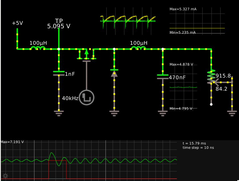
I was thinking about the current-sensing problem today, stimulated by Chris Glaser’s note on high-side current sensing for LED lighting using the voltage drop across the switching power MOSFET. I was driven to revisit a thought I’d had previously about high-side current sensing: if you’re using a microcontroller, maybe you could sense the current intermittently by using an inductor to hold the current constant while you divert it?
Here’s an example of this current-feedback scheme, where the switching P-MOSFET of a standard buck converter is fed from an LC low-pass filter, so its source experiences a significant positive voltage excursion every time it switches off, whose initial slope and peak voltage value should tell us rather precisely how much current the buck converter is drawing.
$ 1 1e-8 0.9487735836358526 50 5 43 5e-11
R -112 -16 -112 -80 0 0 40 5 0 0 0.5
l -112 -16 -16 -16 0 0.00009999999999999999 0.009476973841339323 0
l 112 -16 224 -16 0 0.00009999999999999999 0.007763234883748598 0
f 48 48 48 -16 41 1.5 0.02
w -16 -16 32 -16 0
c -16 -16 -16 96 0 1e-9 4.82585135926864 0.001
g -16 96 -16 128 0 0
R 48 48 48 96 0 2 40000 2.5 2.5 0 0.1
174 336 -16 384 112 1 1000 0.9158000000000001 Resistance
c 224 -16 224 112 0 4.7000000000000005e-7 4.827958335480461 0.001
g 224 112 224 128 0 0
g 384 48 384 128 0 0
w 224 -16 336 -16 0
368 -16 -16 -16 -80 0 0
w 112 -16 64 -16 0
d 112 96 112 -16 2 1N5711
g 112 96 112 128 0 0
403 80 -112 208 -48 0 2_64_0_4103_10_0.1_0_2_2_3
403 240 -112 368 -48 0 12_64_0_4353_5_0.1_0_2_12_3
403 240 16 304 128 0 9_64_0_4354_10_0.05_0_2_9_3
o 13 4 0 4098 10 6.4 0 3 7 0 7 3
In simulation this sort of works, but not as well as I had hoped. When the load is drawing 5.3 mA, the input voltage jounces up to 7.191 V, because at the point the transistor cuts off, the input 100μH inductor is carrying 6.34 mA. But when the load is drawing 50.0 mA, the input voltage jounces up to 9.109 V, because the input inductor was carrying 54.1 mA. Physically this seems wrong; in the 6.34 mA case the inductor holds 2.0 nJ of energy, but the input 1 nF capacitor would contain 25.9 nJ at 7.191 V, while at the nominal 5 V it would contain 12.5 nJ, a gain of a lot more than 2.0 nJ; this could be explained if the voltage on the capacitor was already 6.91 V at the point where the voltage starts climbing. In the 54.1 mA case the 100 μH inductor contains 146 nJ, and at 9.109 V the 1 nF cap contains 41.5 nJ, which is a mystery in the other direction.
This is partly explained by my inept circuit design: I was trying to cut off the P-MOSFET (whose Vth is simulated as -1.5V) by putting its gate at 5 V, but of course as soon as the inductor drives its source up past 6.5 V it starts conducting again. Nevertheless I think it proves out the underlying principle. (This mechanism might actually be a useful way to limit the peak voltage to something safe, if you’re measuring the current using the rate of voltage rise rather than the peak voltage.)
The appeal of this complicated mechanism over a sense resistor (or using the MOSFET on-resistance) is that in theory you should be able to get more precise measurements at lower energy loss and regulation instability for a given precision of voltage measurement.
Suppose your switching MOSFET is a 2N7000: can handle 200 mA (and
dissipate up to 400 mW) and block 60 V with 1.9 Ω of on-resistance,
switched with 2 nC of gate charge with about a 3 V threshold voltage.
(According to Can you get JLCPCB to fabricate a CPU for you affordably from “basic” parts? JLCPCB will solder a 2N7002, a
lower-power version, onto your surface-mount project, for 1.23¢ for
the part plus 0.45¢ for the three terminals. According to file
jellybeans in Dercuano, Digi-Key sells the 2N7002 for 2.958¢ in
quantity 1000, and local merchants here in Argentina sell the 2N7000
for 12¢.) And suppose you’re building a tiny adjustable power supply
with one or more of these, supplying up to 200 mA and up to 12 volts,
working from a 12-volt supply, and you’re using a single-ended ADC
with ±0.2% error over the range 0 to 1.1 volts. (For now I’ll assume
your voltage reference is better than that.)
The 2N7000 has low enough on-resistance that, if it's being operated in the fully-on or fully-off states, it will never come close to its 400 mW limit. The surface-mount 2N7002 has higher on-resistance (7 Ω) and max current (115 mA) but I think is actually more able to dissipate heat than its through-hole progenitor, so I think the max current is the only limit here.
Suppose you’re doing high-side sensing with a 1 Ω sense resistor, just using the ADC directly rather than some kind of differential amplifier or flying-capacitor setup. You need to use some kind of resistive dividers to divide the 12 V signal down into the 1.1 V range, say 100kΩ and 10kΩ (GND-10kΩ-t-100kΩ-x-1Ω-y-100kΩ-u-10kΩ-GND, and the ADC measures the voltages at points t and u in order to measure the current between points x and y). You’ll have some gain error between the two ends of the sense resistor, but that’s easy enough to calibrate out. Then your 200 mA maximum current generates 200 mV, which gets divided down to a difference of 18.2 mV (1.091 V on the high end, 1.073 V on the low end). ±0.2% error on your 1.1 V signal would be ±2.2 mV, which is ±24 mA, or ±12% error on your current reading even at max scale. If you actually care about whether your circuit is using 10 mA or 30 mA, it’s hopeless.
If you use a 4.7Ω sense resistor instead, those 200 mA becomes a 85 mV signal (1.005 V vs. 1.091 V), and your ±0.2% error now translates to ±5.1 mA, which is ±2.5% on your full-range current measurement, which is not good but not completely useless. But such a large sense resistor means that at 200 mA output the sense resistor is eating almost a whole volt; not only is your 12 V circuit running at 11.06 V, if you’re feeding the load 200 mA at 1 V, the high side of the resistor has to be at 1.94 V (and burning 200 mW, which is not good for precision). That’s potentially pretty unhealthy for the load if it suddenly drops from 200 mA to 10 mA — output capacitance upstream of the sense resistor could raise the load voltage up from 1 V to 1.89 V instantly. Capacitance across the load, downstream of the sense resistor, could prevent this, at the cost of creating similar uncontrolled and unmeasured current excursions when the load impedance suddenly drops instead of suddenly rising.
If you use a low-side sense resistor instead, you avoid the need for the 11× divider, and your current-measuring precision correspondingly improves by a factor of 11. This also doubles your data rate and eliminates the need to calibrate out the gain difference between the dividers on the high side and low side of the sense resistor. But now the load isn’t grounded; it’s floating above ground, potentially by as much as 0.94 V in the above 4.7Ω scenario. And the sense resistor is still burning 184 mW at maximum output current. For an isolated supply maybe this doesn’t matter. But this would give us ±0.2% error on the maximum current, i.e. ±400 μA.
Consider instead the situation where we use an LC circuit upstream of the switching transistor. We should be able to arrange for the full-scale C voltage at 12V output to be 48 V or so, and an 0.2% error in measuring that voltage should be 96 mV, which would be an 0.27% error in the 36V ΔV, which corresponds to an 0.54% error on the energy, which corresponds to an 0.27% error in the 200 mA current, ±540 μA. We can take multiple data points on the voltage curve as it rises, which allows us to eliminate any offset error in the ADC, and we don’t have to deal with calibrating out gain differences between different dividers, because we have only one divider to worry about. We could quite plausibly take 20 data points for our measurement with a 1Msps ADC like the one on the STM32 series in 20 μs...
Ugh, but that means that if we want to only be doing this measurement 10% of the time, we can only run the buck converter at 5kHz, which is horrible. I was hoping to come up with a happy story here like "so, you see, we can divert an arbitrarily small amount of our power to measurement, and still get a very precise measurement!" but that's not going to be true with an ADC. So it looks like we’d have to do some analog RF electronics to measure the peak current level. Maybe a flyback winding on the input inductor or something.