I was thinking about building logic out of discrete transistors and other such basic parts.
This is in part driven by JiaLiChuang’s PCB assembly service (see Can you get JLCPCB to fabricate a CPU for you affordably from “basic” parts?). They charge you I think 1.43¢ per PNP transistor, 1.32¢ per NPN transistor, 1.68¢ per N-MOSFET, and 1.79¢ per P-MOSFET, including assembly and soldering, but only 0.35¢ per 0402 resistor or 0.50¢ per 0805 resistor. So a standard CMOS two-input NAND built out of discrete power MOSFETs would be 6.94¢, while a standard RTL two-input NAND would be only 3.69¢, and also use a lot less space.
But can we do better? They only charge you 1.08¢ for a 1N4148W (again, including assembly). The LGP-30 CPU used 113 vacuum tubes and 1450 diodes; the tubes were set up as latches (“flip-flops”) whose set and reset inputs were computed via diode logic. If the vacuum tubes could be replaced by MOSFETs, assembling these parts would cost US$17.56, of which US$1.90 would be the transistors.
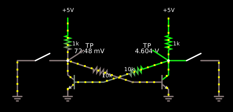
Consider the traditional two-NPN RTL latch. Both NPN transistors have their emitters grounded, base resistors of 10kΩ to the collector of the other transistor, and collector pullups of 1kΩ to Vcc.
$ 1 0.000005 0.8031194996067259 50 5 43 5e-11
t 160 240 80 240 0 1 0.5676806399704408 0.6401601810026045 100 default
t 224 240 304 240 0 1 -4.531171328470282 0.07247958718181605 100 default
g 304 256 304 272 0 0
g 80 256 80 272 0 0
r 160 240 304 192 0 10000
r 224 240 80 192 0 10000
w 80 192 80 224 0
w 304 192 304 224 0
r 80 192 80 112 0 1000
r 304 192 304 112 0 1000
R 304 112 304 80 0 0 40 5 0 0 0.5
R 80 112 80 80 0 0 40 5 0 0 0.5
s 304 192 416 192 0 1 true
g 416 192 416 272 0 0
s -32 192 80 192 0 1 true
g -32 192 -32 272 0 0
368 80 192 128 160 0 0
368 304 192 256 160 0 0
o 16 64 0 4099 5 6.4 0 2 16 3
o 17 64 0 4099 5 6.4 0 2 17 3
Like RTL in general, this sinks current fairly strongly, but sources it fairly weakly. If β = 100 and Vcc = 5 V, the base current is (5 V - 600 mV) / 11kΩ = 400 μA, the transistor on the LOW side of the latch can sink 40 mA while remaining in saturation, but only sinks 5 mA in normal operation. You can flip the latch over by overwhelming it in either direction. By sourcing enough current into its LOW side you can pull it up to HIGH and knock the other side LOW, but this requires about 35 mA (a number which would push it up to 35 V if not restrained by the limited compliance of a current source). By contrast, sinking current from its HIGH side can flip it over with only about 3.9 mA, pushing the collector down by 3.9 V and leaving only 5 - 3.9 - .6 = 0.5 volts across the other transistor’s base resistor, and thus only 50 μA of base current, at which point it desaturates and its Vce starts to soar, flipping the latch back.
This asymmetry is computationally promising: the latch can pull its inputs/outputs down to 0.2 volts sinking 40 mA, but pulling the other output down to 1.1 volts by sinking 3.9 mA is enough to flip the latch’s state. There’s more than a diode drop’s worth of headroom in there and a fanout of about 10, and of course the latch itself provides amplification and inversion:
$ 1 0.000005 0.8031194996067259 50 5 43 5e-11
t 160 240 80 240 0 1 -4.531171328470283 0.07247958718181524 100 default
t 224 240 304 240 0 1 0.5676806399704415 0.6401601810026044 100 default
g 304 256 304 272 0 0
g 80 256 80 272 0 0
r 160 240 304 192 0 10000
r 224 240 80 192 0 10000
w 80 192 80 224 0
w 304 192 304 224 0
r 80 192 80 112 0 1000
r 304 192 304 112 0 1000
R 304 112 304 80 0 0 40 5 0 0 0.5
R 80 112 80 80 0 0 40 5 0 0 0.5
s 304 192 416 192 0 1 true
g 416 192 416 272 0 0
s -32 192 80 192 0 1 true
g -32 192 -32 272 0 0
368 80 192 128 160 0 0
368 304 192 256 160 0 0
368 800 192 752 160 0 0
368 576 192 624 160 0 0
g 464 192 464 272 0 0
s 464 192 576 192 0 1 true
g 912 192 912 272 0 0
s 800 192 912 192 0 1 true
R 576 112 576 80 0 0 40 5 0 0 0.5
R 800 112 800 80 0 0 40 5 0 0 0.5
r 800 192 800 112 0 1000
r 576 192 576 112 0 1000
w 800 192 800 224 0
w 576 192 576 224 0
r 720 240 576 192 0 10000
r 656 240 800 192 0 10000
g 576 256 576 272 0 0
g 800 256 800 272 0 0
t 720 240 800 240 0 1 -4.53117132847028 0.07247958718181717 100 default
t 656 240 576 240 0 1 0.56768063997044 0.6401601810026043 100 default
w 304 192 320 208 0
w 544 208 576 192 0
d 544 208 320 208 2 default
s 80 192 16 128 0 1 true
R 16 128 16 96 0 0 40 5 0 0 0.5
o 16 64 0 4099 5 6.4 0 2 16 3
o 17 64 0 4099 5 6.4 0 2 17 3
o 19 64 0 4099 5 6.4 0 2 19 3
o 18 64 0 4099 5 6.4 0 2 18 3
So by coupling some such latches together with diodes you can compute, among other things, arbitrary logic functions; by releasing a /S signal at some given time you can see whether any of the various sources connected through diodes to its /R input were low at the time, thus computing their AND (in conventional positive logic) and putting their NAND on the /S line at that time.
(The same asymmetry also means you can get 3-stable and 4-stable latches rather than just bistable ones.)
Something I think is more interesting is what happens when you power the latch from a clock signal instead of a constant positive voltage rail. Say the clock signal controls some kind of high-side switch like a PNP transistor; then when the switch is turned off both inputs are basically just 10kΩ to ground (+0.6V at currents above the most minimal) and 2kΩ to each other. The same switch can be shared between probably multiple gates.
If you divide your gates into three phases, you can activate each phase during a different three sixths of a single complete clock cyle:
CK0  CK1  CK2
 *
 *    *
      *
      *    *
           *
 *         *
In this way, gates in phase 1 can compute results from gates in phase 0, gates in phase 2 can compute results from gates in phase 1, and gates in phase 0 can compute results from gates in phase 2.
But how do you ensure a determinate outcome? As before you could release a /R input at a given point during the clock cycle, lengthening the full set of stages within the clock cycle from 6 to 9:
E0 R0 E1 R1 E2 R2
** **
**       **
**    ** **
**    **
      **       **
      **    ** **
      **    **
   **       **
** **       **